
Datasheet

Section 10 I/O Ports
Page 580 of 1384 R01UH0310EJ0500 Rev. 5.00
Sep 25, 2012
H8S/2426, H8S/2426R, H8S/2424 Group
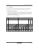
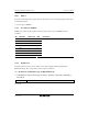
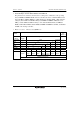
• P52/SCK2/IRQ2-A/BACK-B/PO4-B/TIOCA4-B/TMO0-B
The pin function is switched as shown below according to the combination of the operating
mode, bit EXPE, bit BRLE in BCR of the bus controller, bits OS3 to OS0 in TCSR0 of 8-bit
timer, bits MD3 to MD0 in TMDR_4 of TPU, bits IOA3 to IOA0 in TIOR_4, TPU channel 4
settings by bits CCLR1 and CCLR0 in TCR_4, bit NDER4 in NDERL of PPG, bit C/A in
SMR_2 and bits CKE0 and CKE1 in SCR_2 of the SCI, bits PPGS, TPUS, and TMRS in
PFCR3, bit BACKS in PFCR4, bit P52DDR, bit NDER4 in NDERL of the PPG, and bit ITS2
in ITSR of the interrupt controller.
• Modes 1, 2, and 4 Modes 3 and 7 (EXPE = 1)
BRLE
BACKS
BRLE = 0, or BRLE = 1 and BACKS = 0 BRLE = 1
and
BACKS = 1
TPU channel
4 settings
(1) in table
below
(2) in table below ⎯
OS3 to OS0 ⎯ All 0 Not all 0 ⎯
CKE1 ⎯ 0 1 ⎯ ⎯
C/A ⎯ 0 1 ⎯ ⎯ ⎯
CKE0 ⎯ 0 1 ⎯ ⎯ ⎯ ⎯
P52DDR ⎯ 0 1 1 ⎯ ⎯ ⎯ ⎯ ⎯
NDER4 ⎯ ⎯ 0 1 ⎯ ⎯ ⎯ ⎯ ⎯
P52
input
P52
output
PO4-B
output*
4
SCK2
output
SCK2
output
SCK2
input
TMO0-B
output*
6
BACK-B
output
TIOCA4-B
output*
5
TIOCA4-B input*
1
*
5
Pin function
IRQ2-A interrupt input*
2