
Datasheet

Section 10 I/O Ports
R01UH0310EJ0500 Rev. 5.00 Page 573 of 1384
Sep 25, 2012
H8S/2426, H8S/2426R, H8S/2424 Group
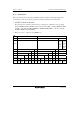
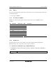
• Modes 3 and 7 (EXPE = 0)
OEE ⎯
OES ⎯
RMTS2 to
RMTS0
⎯
ICE 0 1
CKE1 0 1 ⎯
C/A 0 1 ⎯ ⎯
CKE0 0 1 ⎯ ⎯ ⎯
P35DDR 0 1 ⎯ ⎯ ⎯ ⎯
Pin function P35
input
P35
output
SCK1 output SCK1
output
SCK1
input
SCL0
I/O*
1
Notes: 1. NMOS open-drain output regardless of P35ODR.
2. Not supported in the H8S/2426 and H8S/2424 Groups.
3. Not supported in the 5-V version.
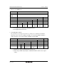
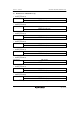
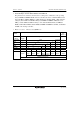
• P34/SCK0/SCK4-A/SDA0
The pin function is switched as shown below according to the combination of bit ICE in
ICCRA_0 of the I
2
C, bit C/A in SMR_0 and SMR_4 of the SCI, bits CKE0 and CKE1 in
SCR_0 and SCR_4 of the SCI, bit SCK4S in PFCR4 and bit P34DDR.
ICE 0 1
CKE1 0 1 ⎯
C/A 0 1 ⎯ ⎯
CKE0 0 1 ⎯ ⎯ ⎯
P34DDR 0 1 ⎯ ⎯ ⎯ ⎯
Pin function P34
input
P34
output
SCK0/SCK4-A
output*
2
*
3
SCK0/SCK4-A
output*
2
*
3
SCK0/SCK4-A
input*
3
SDA0
I/O*
1
Notes: 1. NMOS open-drain output regardless of P34ODR.
2. Simultaneous output of SCK0 and SCK4 cannot be set.
3. When using as SCK4-A input/output, set SCK4S in PFCR4 to 0 before other register
setting.