
Datasheet


Section 10 I/O Ports
R01UH0310EJ0500 Rev. 5.00 Page 563 of 1384
Sep 25, 2012
H8S/2426, H8S/2426R, H8S/2424 Group
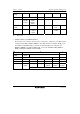
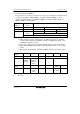
TPU channel 3
settings
(2) (1) (2) (2) (1) (2)
MD3 to MD0 B'0000 B'0010 B'0011
IOD3 to IOD0 B'0000,
B'0100,
B'1xxx
B'0001 to
B'0011,
B'0101 to
B'0111
⎯ B'xx00 Other than B'xx00
CCLR2 to
CCLR0
⎯ ⎯ ⎯ ⎯ Other than
B'110
B'110
Output function ⎯ Output
compare
output
⎯ PWM*
2
mode 1
output
PWM
mode 2
output
⎯
[Legend]
x: Don't care
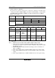
Notes: 1. TIOCA4-A input when MD3 to MD0 = B'0000 or B’01xx and IOA3 to IOA0 = B'10xx.
2. TIOCB4 output disabled.
3. When using as PO4-A output, set PPGS in PFCR3 to 0 before other register setting.
4. When using as TIOCA4-A input/output, set TPUS in PFCR3 to 0 before other register
setting.
5. When using as TMO0-A output, set TMRS in PFCR3 to 0 before other register setting.
6. When using as RxD4-A input, set RXD4S in PFCR4 to 0 before other register setting.