
Datasheet

Section 10 I/O Ports
Page 554 of 1384 R01UH0310EJ0500 Rev. 5.00
Sep 25, 2012
H8S/2426, H8S/2426R, H8S/2424 Group
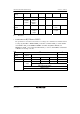
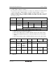
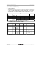
• P24/IRQ12-B/PO4-A/TIOCA4-A/RxD4-A
The pin function is switched as shown below according to the combination of the TPU channel
4 settings (by bits MD3 to MD0 in TMDR_4, bits IOA3 to IOA0 in TIOR_4, and bits CCLR1
and CCLR0 in TCR_4), bit NDER4 in NDERL of the PPG, bit RE in SCR_4 of the SCI, bits
PPGS and TPUS in PFCR3, bit RXD4S in PFCR4, bit P24DDR, and bit ITS12 in ITSR of the
interrupt controller.
TPU channel 4
settings
(1) in table
below
(2) in table below
RE ⎯ 0 1
P24DDR ⎯ 0 1 ⎯
NDER4 ⎯ ⎯ 0 1 ⎯
P24 input P24 output PO4-A output*
4
RxD4-A
input*
6
TIOCA4-A
output*
5
TIOCA4-A input*
1
*
5
Pin function
IRQ12-B interrupt input*
2
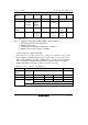
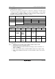
TPU channel 4
settings
(2) (1) (2) (1) (1) (2)
MD3 to MD0 B'0000, B'01xx B'001x B'0010 B'0011
IOA3 to IOA0 B'0000,
B'0100,
B'1xxx
B'0001 to
B'0011,
B'0101 to
B'0111
B'xx00 Other
than B'xx00
Other than B'xx00
CCLR1,
CCLR0
⎯ ⎯ ⎯ ⎯ Other than
B'01
B'01
Output function ⎯ Output
compare output
⎯ PWM*
3
mode 1 output
PWM
mode 2 output
⎯
[Legend]
x: Don't care
Notes: 1. TIOCA4-A input when MD3 to MD0 = B'0000 or B'01xx and IOA3 to IOA0 = B'10xx.
2. IRQ12-B input when the ITS12 bit in ITSR is 1.
3. TIOCB4 output disabled.
4. When using as PO4-A output, set PPGS in PFCR3 to 0 before other register setting.
5. When using as TIOCA4-A input/output, set TPUS in PFCR3 to 0 before other register
setting.
6. When using as RxD4-A input, set RXD4S in PFCR4 to 0 before other register setting.