
Datasheet


Section 10 I/O Ports
Page 550 of 1384 R01UH0310EJ0500 Rev. 5.00
Sep 25, 2012
H8S/2426, H8S/2426R, H8S/2424 Group
10.2.5 Pin Functions
Port 2 pins also function as the pins for PPG outputs, TPU I/Os, interrupt inputs (H8S/2426
Group, H8S/2426R Group), 8-bit timer I/Os (H8S/2424 Group), I
2
C I/Os, and bus control signal
inputs. The correspondence between the register specification and the pin functions is shown
below.
(1) Pin Functions of H8S/2426 Group and H8S/2426R Group
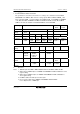
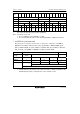
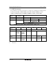
• P27/PO7/TIOCB5/IRQ15-B/SCL2
The pin function is switched as shown below according to the combination of the TPU channel
5 settings (by bits MD3 to MD0 in TMDR_5, bits IOB3 to IOB0 in TIOR_5, and bits CCLR1
and CCLR0 in TCR_5), bit NDER7 in NDERL of the PPG, bit ICE in ICCRA_2 of the I
2
C, bit
P27DDR, and bit ITS15 in ITSR of the interrupt controller.
ICE 0 1
TPU channel 5
settings
(1) in table
below
(2) in table below ⎯
P27DDR ⎯ 0 1 1 ⎯
NDER7 ⎯ ⎯ 0 1 ⎯
P27 input P27 output PO7 output SCL2 I/O*
3
TIOCB5
output
TIOCB5 input*
1
Pin function
IRQ15-B interrupt input*
2
Notes: 1. TIOCB5 input when MD3 to MD0 = B'0000 or B'01xx and IOB3 = 1.
2. IRQ15-B input when the ITS15 bit in ITSR is 1.
3. NMOS open-drain output regardless of P27ODR.