
Datasheet


Section 10 I/O Ports
Page 544 of 1384 R01UH0310EJ0500 Rev. 5.00
Sep 25, 2012
H8S/2426, H8S/2426R, H8S/2424 Group
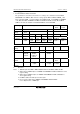
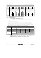
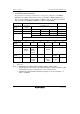
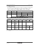
• P12/TEND0/PO10/TIOCC0/TCLKA
The pin function is switched as shown below according to the combination of bit TEE0 in
DMATCR of the DMAC, TPU channel 0 settings (by bits MD3 to MD0 in TMDR_0, bits
IOC3 to IOC0 in TIORL_0, and bits CCLR2 to CCLR0 in TCR_0), bits TPSC2 to TPSC0 in
TCR_0 to TCR_5, bit NDER10 in NDERH of the PPG, and bit P12DDR.
TEE0 0 1
TPU channel 0
settings
(1) in table
below
(2) in table below ⎯
P12DDR ⎯ 0 1 1 ⎯
NDER10 ⎯ ⎯ 0 1 ⎯
P12 input P12 output PO10 output TEND0 output TIOCC0 output
TIOCC0 input*
1
Pin function
TCLKA input*
2
TPU channel 0
settings
(2) (1) (2) (1) (1) (2)
MD3 to MD0 B'0000 B'001x B'0010 B'0011
IOC3 to IOC0 B'0000,
B'0100,
B'1xxx
B'0001 to
B'0011,
B'0101 to
B'0111
B'xx00 Other than
B'xx00
Other than B'xx00
CCLR2 to
CCLR0
⎯ ⎯ ⎯ ⎯ Other than
B'101
B'101
Output function ⎯ Output
compare
output
⎯ PWM*
3
mode 1
output
PWM mode
2 output
⎯
[Legend]
x: Don't care
Notes: 1. TIOCC0 input when MD3 to MD0 = B'0000 and IOC3 to IOC0 = B'10xx.
2. TCLKA input when the setting for any of TCR_0 to TCR_5 is TPSC2 to TPSC0 = B'100.
TCLKA input when phase counting mode is set for channels 1 and 5.
3. TIOCD0 output disabled. Output disabled and settings (2) effective when BFA = 1 or
BFB = 1 in TMDR_0.