
Datasheet


Section 10 I/O Ports
Page 540 of 1384 R01UH0310EJ0500 Rev. 5.00
Sep 25, 2012
H8S/2426, H8S/2426R, H8S/2424 Group
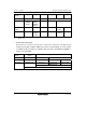
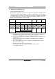
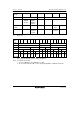
TPU channel 1
settings
(2) (1) (2) (2) (1) (2)
MD3 to MD0 B'0000, B'01xx B'0010 B'0011
IOB3 to IOB0 B'0000,
B'0100,
B'1xxx
B'0001 to
B'0011,
B'0101 to
B'0111
⎯ B'xx00 Other than B'xx00
CCLR1,
CCLR0
⎯ ⎯ ⎯ ⎯ Other than
B'10
B'10
Output function ⎯ Output
compare
output
⎯ ⎯ PWM mode
2 output
⎯
[Legend]
x: Don't care
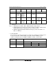
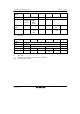
SSU
settings
(1) (1) (3) (3) (2) (1) (2) (1) (1) (1) (1) (2) (1) (2) (2) (1) (2)
SSUMS 0 0 1*
1
BIDE 0 1*
2
0
MSS 0 1 0 1 0 1
TE 0 1 0 1 0 1 0 1 0 1 0 1
RE 0 1 0 1 1 0 1 1 0 1 0 1 0 1 1 0 1
Pin state ⎯ ⎯ SSI
output
SSI
output
SSI
input
⎯ SSI
input
⎯ ⎯ ⎯ ⎯ SSI
input
⎯ SSI
input
SSI
input
⎯ SSI
input
[Legend]
⎯: Not used as the SSU pin (can be used as an I/O port).
Notes: See tables 19.4 to 19.6.
1. Do not set BIDE to 1 when SSUMS = 1 in SSU.
2. Do not specify that TE = RE = 1 when operating with BIDE = 1 (bidirectional mode).