
Datasheet


Section 10 I/O Ports
Page 536 of 1384 R01UH0310EJ0500 Rev. 5.00
Sep 25, 2012
H8S/2426, H8S/2426R, H8S/2424 Group
(2) Pin Functions of H8S/2424 Group
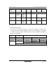
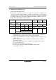
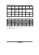
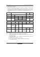
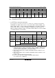
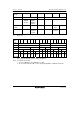
• P17/PO15/TIOCB2/TCLKD/SCS0-A
The pin function is switched as shown below according to the combination of the TPU channel
2 settings (by bits MD3 to MD0 in TMDR_2, bits IOB3 to IOB0 in TIOR_2, and bits CCLR1
and CCLR0 in TCR_2), bits TPSC2 to TPSC0 in TCR_0 and TCR_5, bit NDER15 in NDERH
of the PPG, bits MSS, CSS1, and CSS0 in SSCRH and bit SSUMS in SSCRL of the SSU, bits
SCS0S1 and SCS0S0 in PFCR5, and bit P17DDR.
SSU settings (1) in table below (2) in table
below
(4) in table
below
(3) in table
below
TPU channel 2
settings
(1) in table
below
(2) in table below ⎯
P17DDR ⎯ 0 1 1 0*
6
0*
6
⎯
NDER15 ⎯ ⎯ 0 1 ⎯
P17
input
P17
output
PO15
output
TIOCB2
output
TIOCB2 input*
1
Pin function
TCLKD input*
2
SCS0-A
input*
3
*
7
SCS0-A
I/O*
5
*
7
SCS0-A
output*
4
*
7
Notes: 1. TIOCB2 input when MD3 to MD0 = B'0000 or B'01xx and IOB3 = 1.
2. TCLKD input when the setting for either TCR_0 or TCR_5 is TPSC2 to TPSC0 = B'111.
TCLKD input when channels 2 and 4 are set to phase counting mode.
3. When using as SCS0-A input, set SCS0S1 and SCS0S0 in PFCR5 to B'00 before other
register setting.
4. When using as SCS0-A output, set SCS0S1 and SCS0S0 in PFCR5 to B'00 before
other register setting.
5. When using as SCS0-A input/output, set SCS0S1 and SCS0S0 in PFCR5 to B'00
before other register setting.
6. P17DDR = 0 when the SSU pin is used as input.
7. Do not set up for SSU unless SCS0S1 and SCS0S0 = B'00 in PFCR5.
Use as I/O port or TPU pin.