
Datasheet


Section 10 I/O Ports
R01UH0310EJ0500 Rev. 5.00 Page 527 of 1384
Sep 25, 2012
H8S/2426, H8S/2426R, H8S/2424 Group
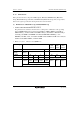
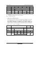
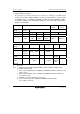
• Modes 3 and 7 (EXPE = 0)
SSU settings (1) in table below (2) in table
below
(3) in table
below
EDRAKE 0 ⎯
TPU channel 2
settings
(1) in table
below
(2) in table below ⎯
P16DDR ⎯ 0 1 1 0*
5
⎯
NDER14 ⎯ ⎯ 0 1 ⎯
P16
input
P16
output
PO14
output
Pin function TIOCA2
output
TIOCA2 input*
1
SSCK0-A
input*
3
*
6
SSCK0-A
output*
4
*
6
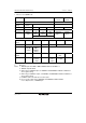
TPU channel 2
settings
(2) (1) (2) (1) (1) (2)
MD3 to MD0 B'0000, B'01xx B'001x B'0010 B'0011
IOA3 to IOA0 B'0000,
B'0100,
B'1xxx
B'0001 to
B'0011,
B'0101 to
B'0111
B'xx00 Other than B'xx00
CCLR1,
CCLR0
⎯ ⎯ ⎯ ⎯ Other than
B'01
B'01
Output function ⎯ Output
compare
output
⎯ PWM*
2
mode 1
output
PWM mode
2 output
⎯
[Legend]
x: Don't care
Notes: 1. TIOCA2 input when MD3 to MD0 = B'0000 or B'01xx and IOA3 = 1.
2. TIOCB2 output disabled.
3. When using as SSCK0-A input, set SSCK0S1 and SSCK0S0 in PFCR5 to B'00 before
other register setting.
4. When using as SSCK0-A output, set SSCK0S1 and SSCK0S0 in PFCR5 to B'00 before
other register setting.
5. P16DDR = 0 when the SSU pin is used as input.
6. Do not set up for SSU unless SSCK0S1 and SSCK0S0 = B'00 in PFCR5.
Use as I/O port, TPU, or EXDMAC pin.