
Datasheet


Section 10 I/O Ports
Page 526 of 1384 R01UH0310EJ0500 Rev. 5.00
Sep 25, 2012
H8S/2426, H8S/2426R, H8S/2424 Group
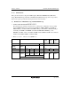
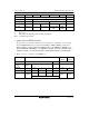
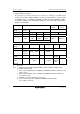
SSU settings (2) (1) (2) (4) (3) (1)
SSUMS 0 1
MSS 0 1 x
CSS1 x 0 1 x
CSS0 x 0 1 0 1 x
Pin state SCS input ⎯ SCS input Automatic SCS
I/O
SCS
output
⎯
[Legend]
x: Don't care
⎯: Not used as the SSU pin (can be used as an I/O port).
Note: See tables 19.4 to 19.6.
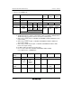
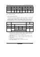
• P16/PO14/TIOCA2/EDRAK2/SSCK0-A
The pin function is switched as shown below according to the combination of the operating
mode, bit EXPE, TPU channel 2 settings (by bits MD3 to MD0 in TMDR_2, bits IOA3 to
IOA0 in TIOR_2, and bits CCLR1 and CCLR0 in TCR_2), bit NDER14 in NDERH of the
PPG, bit EDRAKE in EDMDR_2 of the EXDMAC, bits MSS and SCKS in SSCRH and bit
SSUMS in SSCRL of the SSU, bits SSCK0S1 and SSCK0S0 in PFCR5, and bit P16DDR.
• Modes 1, 2, and 4 Modes 3 and 7 (EXPE = 1)
SSU settings (1) in table below (2) in table
below
(3) in table
below
EDRAKE 0 1 ⎯
TPU channel 2
settings
(1) in table
below
(2) in table below ⎯ ⎯
P16DDR ⎯ 0 1 1 ⎯ 0*
5
⎯
NDER14 ⎯ ⎯ 0 1 ⎯ ⎯
P16 input P16 output PO14
output
EDRAK2
output
Pin function TIOCA2
output
TIOCA2 input*
1
SSCK0-A
input*
3
*
6
SSCK0-A
output*
4
*
6