
Datasheet

Section 10 I/O Ports
R01UH0310EJ0500 Rev. 5.00 Page 507 of 1384
Sep 25, 2012
H8S/2426, H8S/2426R, H8S/2424 Group
Section 10 I/O Ports
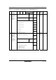
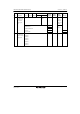
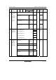
Table 10.1 summarizes the port functions of the H8S/2426 Group and H8S/2426R Group. Table
10.2 summarizes the port functions of the H8S/2424 Group. The pins of each port also have other
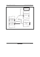
functions such as input/output or external interrupt input pins of on-chip peripheral modules. Each
I/O port includes a data direction register (DDR) that controls input/output, a data register (DR)
that stores output data, a port register (PORT) used to read the pin states, and a port function
control register (PFCR) used to set input/output destination. Before enabling each input/output
pins, select the input/output destination by PFCR. The input-only ports do not have a DR or DDR
register.
Ports A to E have a built-in pull-up MOS function and a pull-up MOS control register (PCR) to
control the on/off state of the input pull-up MOS.
Ports 1 to 3, 5 to 8, and A to J include an open-drain control register (ODR) that controls the
on/off state of the output buffer PMOS.
Ports 1 to 3 and 5 to 8 can drive a single TTL load and 30-pF capacitive load. Ports A to J can
drive a single TTL load and 50-pF capacitive load.
All of the I/O ports can drive a Darlington transistor when outputting data.
Ports 1 and 2 are Schmitt-triggered inputs. The other ports are Schmitt-triggered inputs when used
as IRQ inputs, 16-bit timer pulse unit (TPU) inputs, 8-bit timer (TMR) inputs, and I
2
C bus
interface (IIC) inputs.