
Datasheet

Section 9 Data Transfer Controller (DTC)
R01UH0310EJ0500 Rev. 5.00 Page 501 of 1384
Sep 25, 2012
H8S/2426, H8S/2426R, H8S/2424 Group
9.7 Examples of Use of the DTC
9.7.1 Normal Mode
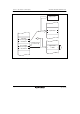
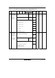
An example is shown in which the DTC is used to receive 128 bytes of data via the SCI.
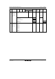
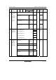
1. Set MRA to fixed source address (SM1 = SM0 = 0), incrementing destination address (DM1 =
1, DM0 = 0), normal mode (MD1 = MD0 = 0), and byte size (Sz = 0). The DTS bit can have
any value. Set MRB for one data transfer by one interrupt (CHNE = 0, DISEL = 0). Set the
SCI RDR address in SAR, the start address of the RAM area where the data will be received in
DAR, and 128 (H'0080) in CRA. CRB can be set to any value.
2. Set the start address of the register information at the DTC vector address.
3. Set the corresponding bit in DTCER to 1.
4. Set the SCI to the appropriate receive mode. Set the RIE bit in SCR to 1 to enable the
reception complete (RXI) interrupt. Since the generation of a receive error during the SCI
reception operation will disable subsequent reception, the CPU should be enabled to accept
receive error interrupts.
5. Each time reception of one byte of data ends on the SCI, the RDRF flag in SSR is set to 1, an
RXI interrupt is generated, and the DTC is activated. The receive data is transferred from RDR
to RAM by the DTC. DAR is incremented and CRA is decremented. The RDRF flag is
automatically cleared to 0.
6. When CRA becomes 0 after the 128 data transfers have ended, the RDRF flag is held at 1, the
DTCE bit is cleared to 0, and an RXI interrupt request is sent to the CPU. The interrupt
handling routine should perform wrap-up processing.