
Datasheet

Section 9 Data Transfer Controller (DTC)
Page 488 of 1384 R01UH0310EJ0500 Rev. 5.00
Sep 25, 2012
H8S/2426, H8S/2426R, H8S/2424 Group
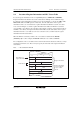
Origin of
Activation
Source
Activation
Source
Vector
Number
DTC Vector
Address
DTCE*
1
Priority
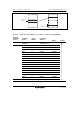
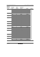
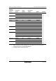
SCI_3 RXI3 101 H'04CA DTCEF5 High
TXI3 102 H'04CC DTCEF4
SCI_4 RXI4 105 H'04D2 DTCEG3
TXI4 106 H'04D4 DTCEG2
A/D_1 ADI1 112 H'04E0 DTCEG1
TPU_6 TGI6A 120 H'04F0 DTCEG0
TGI6B 121 H'04F2 DTCEH7
TGI6C 122 H'04F4 DTCEH6
TGI6D 123 H'04F6 DTCEH5
TPU_7 TGI7A 125 H'04FA DTCEH4
TGI7B 126 H'04FC DTCEH3
TPU_8 TGI8A 129 H'0502 DTCEH2
TGI8B 130 H'0504 DTCEH1
TPU_9 TGI9A 133 H'050A DTCEH0
TGI9B 134 H'050C DTCEI7
TGI9C 135 H'050E DTCEI6
TGI9D 136 H'0510 DTCEI5
TPU_10 TGI10A 138 H'0514 DTCEI4
TGI10B 139 H'0516 DTCEI3
TPU_11 TGI11A 142 H'051C DTCEI2
TGI11B 143 H'051E DTCEI1 Low
Notes: 1. DTCE bits with no corresponding interrupt are reserved, and 0 should be written to.
When clearing the software standby state or all-module-clocks-stop mode with an
interrupt, write 0 to the corresponding DTCE bit.
2. Not supported by the H8S/2424 Group.