
Datasheet


Section 8 EXDMA Controller (EXDMAC)
R01UH0310EJ0500 Rev. 5.00 Page 453 of 1384
Sep 25, 2012
H8S/2426, H8S/2426R, H8S/2424 Group
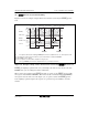
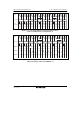
(4) EDREQ Pin Low Level Activation Timing
Figure 8.27 shows an example of single address mode transfer activated by the EDREQ pin low
level.
Single Single
EXDMA
single cycle
Address bus
φ
EDREQ
Idle
Bus release
EXDMA control
Channel
Transfer source/
destination
Transfer source/
destination
Bus release
Idle
Bus release
Idle
EDACK
[1] [3][2] [4] [6][5] [7]
Acceptance
resumed
Acceptance
resumed
Request
clearance period
Request
clearance period
Request Request
Minimum 3 cycles Minimum 3 cycles
[1] Acceptance after transfer enabling; EDREQ pin low level is sampled at rise of φ, and request is held.
[2], [5] Request is cleared at end of next bus cycle, and activation is started in EXDMAC.
[3], [6] EXDMA cycle is started.
[4], [7] Acceptance is resumed after completion of single cycle.
(As in [1], EDREQ pin low level is sampled at rise of φ, and request is held.)
EXDMA
single cycle
Figure 8.27 Example of Single Address Mode Transfer Activated by EDREQ Pin Low Level
EDREQ pin sampling is performed in each cycle starting at the next rise of φ after the end of the
EDMDR write cycle for setting the transfer-enabled state.
When a low level is sampled at the EDREQ pin while acceptance via the EDREQ pin is possible,
the request is held within the EXDMAC. Then when activation is initiated within the EXDMAC,
the request is cleared. At the end of the single cycle, acceptance resumes and EDREQ pin low
level sampling is performed again; this sequence of operations is repeated until the end of the
transfer.