
Datasheet

Section 7 DMA Controller (DMAC)
R01UH0310EJ0500 Rev. 5.00 Page 393 of 1384
Sep 25, 2012
H8S/2426, H8S/2426R, H8S/2424 Group
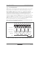
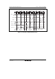
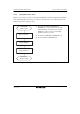
Figure 7.33 shows an example of single address transfer using the write data buffer function. In
this example, the CPU program area is in on-chip memory.
Internal address
φ
Internal read signal
RD
DACK
External address
DMA
read
DMA
single
CPU
read
DMA
single
CPU
read
Figure 7.33 Example of Single Address Transfer Using Write Data Buffer Function
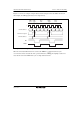
When the write data buffer function is activated, the DMAC recognizes that the bus cycle
concerned has ended, and starts the next operation. Therefore, DREQ pin sampling is started one
state after the start of the DMA write cycle or single address transfer.