
Datasheet

Section 6 Bus Controller (BSC)
Page 304 of 1384 R01UH0310EJ0500 Rev. 5.00
Sep 25, 2012
H8S/2426, H8S/2426R, H8S/2424 Group
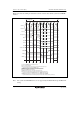
6.11 Write Data Buffer Function
This LSI has a write data buffer function for the external data bus. Using the write data buffer
function enables external writes and DMA single address mode transfers to be executed in parallel
with internal accesses. The write data buffer function is made available by setting the WDBE bit
to 1 in BCR.
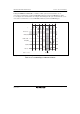
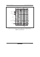
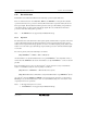
Figure 6.95 shows an example of the timing when the write data buffer function is used. When this
function is used, if an external address space write or DMA single address mode transfer continues
for two states or longer, and there is an internal access next, an external write only is executed in
the first state, but from the next state onward an internal access (on-chip memory or internal I/O
register read/write) is executed in parallel with the external address space write rather than waiting
until it ends.
T
1
Internal address bus
A23 to A0
External write cycle
HWR, LWR
T
2
T
W
T
W
T
3
On-chip memory read Internal I/O register read
Internal read signal
CSn
D15 to D0
External address
Internal memory
External space
write
Internal I/O register address
φ
Figure 6.95 Example of Timing when Write Data Buffer Function Is Used