
Datasheet


Section 6 Bus Controller (BSC)
Page 294 of 1384 R01UH0310EJ0500 Rev. 5.00
Sep 25, 2012
H8S/2426, H8S/2426R, H8S/2424 Group
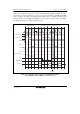
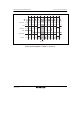
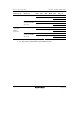
(7) Idle Cycle in Case of Normal Space Access after DRAM Space Access
Note: The DRAM interface is not supported by the 5-V version.
(a) Normal space access after DRAM space read access
While the DRMI bit is cleared to 0 in DRACCR, idle cycle insertion after DRAM space access is
disabled. Idle cycle insertion after DRAM space access can be enabled by setting the DRMI bit to
1. The conditions and number of states of the idle cycle to be inserted are in accordance with the
settings of bits ICIS1, ICIS0, and IDLC in BCR are valid. Figures 6.88 and 6.89 show examples of
idle cycle operation when the DRMI bit is set to 1.
When the DRMI bit is cleared to 0, an idle cycle is not inserted after DRAM space access even if
bits ICIS1 and ICIS0 are set to 1.
T
p
Address bus
φ
RD
RAS
U
CAS, LCAS
External address space read
Idle cycle
Data bus
T
r
T
c1
T
c2
T
1
DRAM space readDRAM space read
T
2
T
c2
T
3
T
i
T
i
T
c1
Figure 6.88 Example of Idle Cycle Operation after DRAM Access
(Consecutive Reads in Different Areas) (IDLC = 0, RAST = 0, CAST = 0)