
Datasheet


Section 6 Bus Controller (BSC)
Page 290 of 1384 R01UH0310EJ0500 Rev. 5.00
Sep 25, 2012
H8S/2426, H8S/2426R, H8S/2424 Group
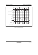
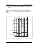
(6) Idle Cycle in Case of Continuous Synchronous DRAM Space Access after Normal
Space Access
In a continuous synchronous DRAM space access following a normal space access, the settings of
bits ICIS2, ICIS1, ICIS0, and IDLC in BCR are valid. However, in the case of consecutive reads
in different areas, for example, if the second read is a full access to continuous synchronous
DRAM space, only Tp cycle is inserted, and Ti cycle is not. The timing in this case is shown in
figure 6.84.
Note: The synchronous DRAM interface is not supported by the H8S/2426 Group and H8S/2424
Group.
T
1
Address bus
φ
Column address
Row
address
Row
address
Column
address
Data bus
T
2
T
3
T
p
T
r
T
c2
External space read Synchronous DRAM space read
T
cl
T
c1
RAS
CAS
WE
RD
CKE
PALL ACTV
NOPNOP READ
DQMU, DQML
Precharge-sel
Figure 6.84 Example of Synchronous DRAM Full Access after External Read
(CAS Latency 2)