
Datasheet


Section 6 Bus Controller (BSC)
Page 284 of 1384 R01UH0310EJ0500 Rev. 5.00
Sep 25, 2012
H8S/2426, H8S/2426R, H8S/2424 Group
6.10 Idle Cycle
6.10.1 Operation
When this LSI accesses external address space, it can insert an idle cycle (T
i
) between bus cycles
in the following three cases: (1) when read accesses in different areas occur consecutively, (2)
when a write cycle occurs immediately after a read cycle, and (3) when a read cycle occurs
immediately after a write cycle. Insertion of a 1-state or 2-state idle cycle can be selected with the
IDLC bit in BCR. By inserting an idle cycle it is possible, for example, to avoid data collisions
between ROM, etc., with a long output floating time, and high-speed memory, I/O interfaces, and
so on.
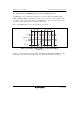
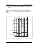
(1) Consecutive Reads in Different Areas
If consecutive reads in different areas occur while the ICIS1 bit is set to 1 in BCR, an idle cycle is
inserted at the start of the second read cycle.
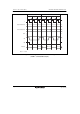
Figure 6.77 shows an example of the operation in this case. In this example, bus cycle A is a read
cycle for ROM with a long output floating time, and bus cycle B is a read cycle for SRAM, each
being located in a different area. In (a), an idle cycle is not inserted, and a collision occurs in bus
cycle B between the read data from ROM and that from SRAM. In (b), an idle cycle is inserted,
and a data collision is prevented.
T
1
Address bus
φ
RD
Bus cycle A
Data bus
T
2
T
3
T
1
T
2
Bus cycle B
Long output floating time
Data collision
(a) No idle cycle insertion
(ICIS1 = 0)
T
1
Address bus
φ
RD
Bus cycle A
Data bus
T
2
T
3
T
i
T
1
Bus cycle B
(b) Idle cycle insertion
(ICIS1 = 1, initial value)
T
2
CS (area A)
CS (area B)
CS (area A)
CS (area B)
Idle cycle
Figure 6.77 Example of Idle Cycle Operation
(Consecutive Reads in Different Areas)