
Datasheet


Section 6 Bus Controller (BSC)
R01UH0310EJ0500 Rev. 5.00 Page 283 of 1384
Sep 25, 2012
H8S/2426, H8S/2426R, H8S/2424 Group
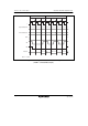
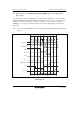
T
1
Upper address bus
Lower address bus
φ
CSn
AS
Data bus
T
2
T
1
T
1
Full access
RD
Burst access
Note: n = 1 and 0
Figure 6.76 Example of Burst ROM Access Timing
(ASTn = 0, 1-State Burst Cycle)
6.9.2 Wait Control
As with the basic bus interface, either program wait insertion or pin wait insertion using the WAIT
pin can be used in the initial cycle (full access) on the burst ROM interface. See section 6.5.4,
Wait Control. Wait states cannot be inserted in a burst cycle.
6.9.3 Write Access
When a write access to burst ROM space is executed, burst access is interrupted at that point and
the write access is executed in line with the basic bus interface settings. Write accesses are not
performed in burst mode even though burst ROM space is designated.