
Datasheet


Section 6 Bus Controller (BSC)
Page 270 of 1384 R01UH0310EJ0500 Rev. 5.00
Sep 25, 2012
H8S/2426, H8S/2426R, H8S/2424 Group
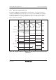
T
Rp
SDRAMφ
RAS
CAS
WE
CKE
PALL NOPREF
A
ddress bus
T
Rr
T
Rc1
T
Rc2
Precharge-sel
High
φ
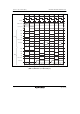
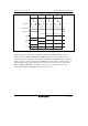
Figure 6.66 Auto Refresh Timing
When the interval specification from the PALL command to the REF command cannot be
satisfied, setting the RCW1 and RCW0 bits of REFCR enables one to three wait states to be
inserted after the T
Rp
cycle that is set by the TPC1 and TPC0 bits of DRACCR. Set the optimum
number of waits according to the synchronous DRAM connected and the operating frequency of
this LSI. Figure 6.67 shows the timing when one wait state is inserted. Since the setting of bits
TPC1 and TPC0 of DRACCR is also valid in refresh cycles, the command interval can be
extended by the RCW1 and RCW0 bits after the precharge cycles.