
Datasheet


Section 6 Bus Controller (BSC)
R01UH0310EJ0500 Rev. 5.00 Page 265 of 1384
Sep 25, 2012
H8S/2426, H8S/2426R, H8S/2424 Group
6.8.12 Burst Operation
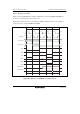
With synchronous DRAM, in addition to full access (normal access) in which data is accessed by
outputting a row address for each access, burst access is also provided which can be used when
making consecutive accesses to the same row address. This access enables fast access of data by
simply changing the column address after the row address has been output. Burst access can be
selected by setting the BE bit to 1 in DRAMCR.
DQM has the 2-cycle latency when synchronous DRAM is read. Therefore, the DQM signal
cannot be specified to the Tc2 cycle data output if the Tc1 cycle is executed for second or
following column address when the CAS latency is set to 1 to issue the READ command. Do not
set the BE bit to 1 when synchronous DRAM of CAS latency 1 is connected.
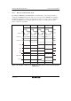
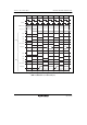
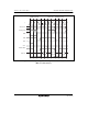
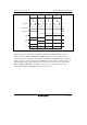
(1) Burst Access Operation Timing
Figure 6.64 shows the operation timing for burst access. When there are consecutive access cycles
for continuous synchronous DRAM space, the column address output cycles continue as long as
the row address is the same for consecutive access cycles. The row address used for the
comparison is set with bits MXC2 to MXC0 in DRAMCR.