
Datasheet


Section 6 Bus Controller (BSC)
Page 264 of 1384 R01UH0310EJ0500 Rev. 5.00
Sep 25, 2012
H8S/2426, H8S/2426R, H8S/2424 Group
This LSI
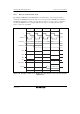
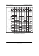
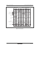
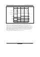
(Address shift size set to 8 bits)
CS2 (RAS)
CS3 (CAS)
CS4 (WE)
16-Mbit synchronous DRAM
1 Mword × 16 bits × 4-bank configuration
8-bit column address
RAS
CAS
WE
UCAS (DQMU)
LCAS (DQML)
A9 A8
A10 A9
A8 A7
A12 A11
Notes: 1. Bank control is not available.
2. The CKE and CS pins must be fixed to 1 when the power supply is input.
3. The CS pin must be fixed to 0 before accessing synchronous DRAM.
A21
A12 (BS0)
A23
A13 (BS1)
CS5 (SDRAM
φ
)
CLK
DQML
DQMU
A11 A10
A7 A6
A6 A5
A5 A4
A4 A3
A3 A2
A2 A1
A1
I/O PORT
A0
D15 to D0 DQ15 to DQ0
OE (CKE) CKE
CS
Row address
input: A11 to A0
Column address
input: A7 to A0
Bank select
address: A13/A12
Figure 6.63 Example of DQMU and DQML Byte Control