
Datasheet


Section 6 Bus Controller (BSC)
R01UH0310EJ0500 Rev. 5.00 Page 253 of 1384
Sep 25, 2012
H8S/2426, H8S/2426R, H8S/2424 Group
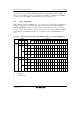
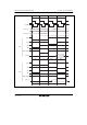
Table 6.10 Synchronous DRAM Interface Pins
Pin
With
Synchronous
DRAM Setting
Name I/O Function
CS2 RAS Row address strobe Output Row address strobe when
areas 2 to 5 are designated
as continuous synchronous
DRAM space
CS3 CAS Column address strobe Output Column address strobe when
areas 2 to 5 are designated
as continuous synchronous
DRAM space
CS4 WE Write enable Output Write enable strobe when
areas 2 to 5 are designated
as continuous synchronous
DRAM space
CS5 SDRAMφ Clock Output Clock only for synchronous
DRAM
(OE) (CKE) Clock enable Output Clock enable signal when
areas 2 to 5 are designated
as continuous synchronous
DRAM space
UCAS DQMU Upper data mask enable Output Upper data mask enable for
16-bit continuous
synchronous DRAM space
access/data mask enable for
8-bit continuous synchronous
DRAM space access
LCAS DQML Lower data mask enable Output Lower data mask enable
signal for 16-bit continuous
synchronous DRAM space
access
A15 to A0 A15 to A0 Address pins Output Row address/column address
multiplexed output pins
D15 to D0 D15 to D0 Data pins I/O Data input/output pins