
Datasheet


Section 6 Bus Controller (BSC)
R01UH0310EJ0500 Rev. 5.00 Page 251 of 1384
Sep 25, 2012
H8S/2426, H8S/2426R, H8S/2424 Group
Commands that are supported by this LSI are NOP, auto-refresh (REF), self-refresh (SELF), all
bank precharge (PALL), row address strobe bank-active (ACTV), read (READ), write (WRIT),
and mode-register write (MRS). Commands for bank control cannot be used.
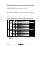
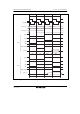
6.8.2 Address Multiplexing
With continuous synchronous DRAM space, the row address and column address are multiplexed.
In address multiplexing, the size of the shift of the row address is selected with bits MXC2 to
MXC0 in DRAMCR. The address-precharge-setting command (Precharge-sel) can be output on
the upper column address. Table 6.9 shows the relation between the settings of MXC2 to MXC0
and the shift size. The MXC2 bit should be set to 1 when the synchronous DRAM interface is
used.
Table 6.9 Relation between Settings of Bits MXC2 to MXC0 and Address Multiplexing
DRAMCR Address Pins
MXC2 MXC1 MXC0
Shift
Size
A23 to
A16
A15 A14 A13 A12 A11 A10 A9 A8 A7 A6 A5 A4 A3 A2 A1 A0
0 x x Reserved (setting prohibited)
0 8
bits
A23 to
A16
A23 A22 A21 A20 A19 A18 A17 A16 A15 A14 A13 A12 A11 A10 A9 A8 0
1 9
bits
A23 to
A16
A15 A23 A22 A21 A20 A19 A18 A17 A16 A15 A14 A13 A12 A11 A10 A9
0 10
bits
A23 to
A16
A15 A14 A23 A22 A21 A20 A19 A18 A17 A16 A15 A14 A13 A12 A11 A10
Row
address
1
1
1 11
bits
A23 to
A16
A15 A14 A13 A23 A22 A21 A20 A19 A18 A17 A16 A15 A14 A13 A12 A11
0 × × Reserved (setting prohibited)
0 ⎯ A23 to
A16
P P P P P P P A8 A7 A6 A5 A4 A3 A2 A1 A0 0
1 ⎯ A23 to
A16
P P P P P P A9 A8 A7 A6 A5 A4 A3 A2 A1 A0
0 ⎯ A23 to
A16
P P P P P A10 A9 A8 A7 A6 A5 A4 A3 A2 A1 A0
Column
address
1
1
1 ⎯ A23 to
A16
P P P P A11 A10 A9 A8 A7 A6 A5 A4 A3 A2 A1 A0
[Legend]
x: Don't care.
P: Precharge-sel