
Datasheet


Section 6 Bus Controller (BSC)
R01UH0310EJ0500 Rev. 5.00 Page 247 of 1384
Sep 25, 2012
H8S/2426, H8S/2426R, H8S/2424 Group
(3) Refreshing and All-Module-Clocks-Stopped Mode
In this LSI, if the ACSE bit is set to 1 in MSTPCRH, and then a SLEEP instruction is executed
with the setting for all peripheral module clocks to be stopped (MSTPCR = H'FFFF, EXMSTPCR
= H'FFFF) or for operation of the 8-bit timer module alone (MSTPCR = H'FFFE, EXMSTPCR =
H'FFFF), and a transition is made to the sleep state, the all-module-clocks-stopped mode is
entered, in which the bus controller and I/O port clocks are also stopped. As the bus controller
clock is also stopped in this mode, CBR refreshing is not executed. If DRAM is connected
externally and DRAM data is to be retained in sleep mode, the ACSE bit must be cleared to 0 in
MSTPCRH.
6.7.13 DMAC and EXDMAC Single Address Transfer Mode and DRAM Interface
When burst mode is selected on the DRAM interface, the DACK and EDACK output timing can
be selected with the DDS and EDDS bits in DRAMCR. When DRAM space is accessed in DMAC
or EXDMAC single address mode at the same time, these bits select whether or not burst access is
to be performed.
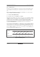
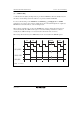
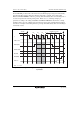
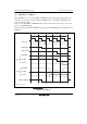
(1) When DDS = 1 or EDDS = 1
Burst access is performed by determining the address only, irrespective of the bus master. With
the DRAM interface, the DACK or EDACK output goes low from the T
c1
state.
Figure 6.53 shows the DACK or EDACK output timing for the DRAM interface when DDS = 1 or
EDDS = 1.