
Datasheet


Section 6 Bus Controller (BSC)
Page 230 of 1384 R01UH0310EJ0500 Rev. 5.00
Sep 25, 2012
H8S/2426, H8S/2426R, H8S/2424 Group
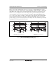
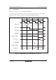
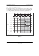
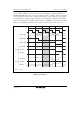
6.7.8 Precharge State Control
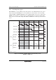
When DRAM is accessed, a RAS precharge time must be secured. With this LSI, one T
p
state is
always inserted when DRAM space is accessed. From one to four T
p
states can be selected by
setting bits TPC1 and TPC0 in DRACCR. Set the optimum number of T
p
cycles according to the
DRAM connected and the operating frequency of this LSI. Figure 6.37 shows the timing when
two T
p
states are inserted. The setting of bits TPC1 and TPC0 is also valid for T
p
states in refresh
cycles.
T
p1
RASn (CSn)
Read
Write
UCAS, LCAS
WE (HWR)
OE (RD)
Data bus
WE (HWR)
OE (RD)
Data bus
Address bus
φ
T
p2
T
r
T
c1
T
c2
Row address Column address
High
High
Note: n = 2 to 5
Figure 6.37 Example of Timing with Two-State Precharge Cycle
(RAST = 0, CAST = 0)