
Datasheet


Section 6 Bus Controller (BSC)
Page 228 of 1384 R01UH0310EJ0500 Rev. 5.00
Sep 25, 2012
H8S/2426, H8S/2426R, H8S/2424 Group
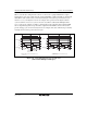
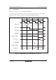
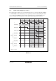
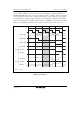
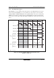
6.7.7 Row Address Output State Control
If the RAST bit is set to 1 in DRAMCR, the RAS signal goes low from the beginning of the T
r
state, and the row address hold time and DRAM read access time are changed relative to the fall of
the RAS signal. Use the optimum setting according to the DRAM connected and the operating
frequency of this LSI. Figure 6.35 shows an example of the timing when the RAS signal goes low
from the beginning of the T
r
state.
T
p
RASn (CSn)
Read
Write
UCAS, LCAS
WE (HWR)
OE (RD)
Data bus
WE (HWR)
OE (RD)
Data bus
Address bus
φ
T
r
T
c1
T
c2
Row address Column address
High
High
Note: n = 2 to 5
Figure 6.35 Example of Access Timing when RAS Signal Goes Low from Beginning
of T
r
State (CAST = 0)