
Datasheet


Section 6 Bus Controller (BSC)
Page 224 of 1384 R01UH0310EJ0500 Rev. 5.00
Sep 25, 2012
H8S/2426, H8S/2426R, H8S/2424 Group
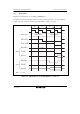
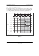
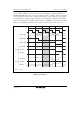
6.7.4 Pins Used for DRAM Interface
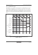
Table 6.7 shows the pins used for DRAM interfacing and their functions.
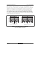
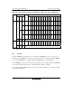
Table 6.7 DRAM Interface Pins
Pin
With DRAM
Setting Name I/O Function
HWR WE Write enable Output Write enable for DRAM space
access
CS2 RAS2 Row address strobe 2 Output Row address strobe when area
2 is designated as DRAM space
or row address strobe when
areas 2 to 5 are designated as
continuous DRAM space
CS3 RAS3 Row address strobe 3 Output Row address strobe when area
3 is designated as DRAM space
CS4 RAS4 Row address strobe 4 Output Row address strobe when area
4 is designated as DRAM space
CS5 RAS5 Row address strobe 5 Output Row address strobe when area
5 is designated as DRAM space
UCAS UCAS Upper column address
strobe
Output Upper column address strobe for
16-bit DRAM space access or
column address strobe for 8-bit
DRAM space access
LCAS LCAS Lower column address
strobe
Output Lower column address strobe
signal for 16-bit DRAM space
access
RD, OE OE Output enable Output Output enable signal for DRAM
space access
WAIT WAIT Wait Input Wait request signal
A15 to A0 A15 to A0 Address pins Output Row address/column address
multiplexed output
D15 to D0 D15 to D0 Data pins I/O Data input/output pins