
Datasheet


Section 6 Bus Controller (BSC)
Page 220 of 1384 R01UH0310EJ0500 Rev. 5.00
Sep 25, 2012
H8S/2426, H8S/2426R, H8S/2424 Group
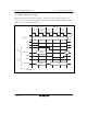
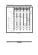
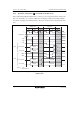
6.6.8 Extension of Chip Select (CS) Assertion Period in Data Cycle
In the address/data multiplexed I/O interface, extension cycles can be inserted before and after the
data cycle. For details, see section 6.5.6, Extension of Chip Select (CS) Assertion Period. Figure
6.31 shows an example of the timing when the chip select assertion period is extended in the data
cycle.
CSn
HWR
LWR
AH
RD
AD15 to AD8
AD7 to AD0
AD15 to AD8
AD7 to AD0
Tma1 Th T1 T2 Tt
Tma2
Address cycle Data cycle
φ
Address bus
Write
Read
Address
Address
Read
data
Write data
Notes: 1. n = 6, 7
2. When RDNn = 0
Address
Address
Read
data
Write data
Figure 6.31 Example of Timing when Chip Select Assertion Period Is Extended
in Data Cycle