
Datasheet


Section 6 Bus Controller (BSC)
Page 208 of 1384 R01UH0310EJ0500 Rev. 5.00
Sep 25, 2012
H8S/2426, H8S/2426R, H8S/2424 Group
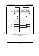
Both extension state T
h
inserted before the basic bus cycle and extension state T
t
inserted after the
basic bus cycle, or only one of these, can be specified for individual areas. Insertion or non-
insertion can be specified for the T
h
state with the upper 8 bits (CSXH7 to CSXH0) in the CSACR
register, and for the T
t
state with the lower 8 bits (CSXT7 to CSXT0).
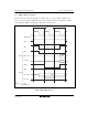
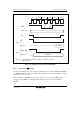
6.6 Address/Data Multiplexed I/O Interface
If areas 6 and 7 of the external address space are specified as address/data multiplexed I/O space
in this LSI, the address/data multiplexed I/O interfacing can be performed. In the address/data
multiplexed I/O interface, peripheral LSIs that require address/data multiplexing can be connected
directly to this LSI.
6.6.1 Setting Address/Data Multiplexed I/O Space
In the address/data multiplexed I/O interface, areas 6 and 7 are designated as the address/data
multiplexed I/O space by setting the MPXE bit in MPXCR to 1.
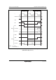
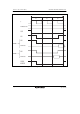
6.6.2 Address/Data Multiplexing
With the address/data multiplexed I/O space, the data bus and address bus are multiplexed. Table
6.4 shows the relation between the bus width and corresponding address output.
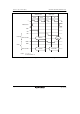
Table 6.4 Multiplexed Address/Data
Data Pins
Bus
Width
Cycle AD15 AD14 AD13 AD12 AD11 AD10 AD9 AD8 AD7 AD6 AD5 AD4 AD3 AD2 AD1 AD0
Address
A7 A6 A5 A4 A3 A2 A1 A0 ⎯ ⎯ ⎯ ⎯ ⎯ ⎯ ⎯ ⎯
8 bits
Data
D15 D14 D13 D12 D11 D10 D9 D8 ⎯ ⎯ ⎯ ⎯ ⎯ ⎯ ⎯ ⎯
Address
A15 A14 A13 A12 A11 A10 A9 A8 A7 A6 A5 A4 A3 A2 A1 A0
16 bits
Data
D15 D14 D13 D12 D11 D10 D9 D8 D7 D6 D5 D4 D3 D2 D1 D0