
Datasheet


Section 6 Bus Controller (BSC)
R01UH0310EJ0500 Rev. 5.00 Page 191 of 1384
Sep 25, 2012
H8S/2426, H8S/2426R, H8S/2424 Group
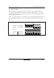
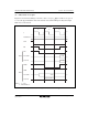
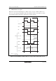
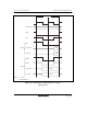
6.4.4 Chip Select Signals
This LSI can output chip select signals (CS0 to CS7) for areas 0 to 7. The signal outputs low when
the corresponding external space area is accessed. Figure 6.7 shows an example of CS0 to CS7
signals output timing.
Enabling or disabling of CS0 to CS7 signals output is set by the data direction register (DDR) bit
for the port corresponding to the CS0 to CS7 pins.
In expanded mode with on-chip ROM disabled, the CS0 pin is placed in the output state after a
reset. Pins CS1 to CS7 are placed in the input state after a reset and so the corresponding DDR bits
and PFCR0 bits should be set to 1 when outputting signals CS1 to CS7.
In expanded mode with on-chip ROM enabled, pins CS0 to CS7 are all placed in the input state
after a reset and so the corresponding DDR bits and PFCR0 bits should be set to 1 when
outputting signals CS0 to CS7.
When areas 2 to 5 are designated as DRAM*
1
space, outputs CS2 to CS5 are used as RAS2 to
RAS5 signals, and when designated as continuous DRAM space, the CS2 output is used as the
RAS signal.
When areas 2 to 5 are designated as continuous synchronous DRAM*
2
space in the H8S/2426R
Group, outputs CS2, CS3, CS4, and CS5 are used as RAS, CAS, WE, and CLK signals.
Notes: The A23E bit in PFCR1 should be cleared to 0 when CS7 signal is output in the H8S/2424
Group.
1. The DRAM interface is not supported by the 5-V version.
2. The synchronous DRAM interface is not supported by the H8S/2426 Group and
H8S/2424 Group.