
Datasheet


Section 6 Bus Controller (BSC)
R01UH0310EJ0500 Rev. 5.00 Page 183 of 1384
Sep 25, 2012
H8S/2426, H8S/2426R, H8S/2424 Group
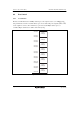
Bit Bit Name Initial Value R/W Description
11 ⎯ 0 R/W Reserved
This bit can be read from or written to. However,
the write value should always be 0.
10
9
8
RTCK2
RTCK1
RTCK0
0
0
0
R/W
R/W
R/W
Refresh Counter Clock Select
These bits select the clock to be used to
increment the refresh counter. When the input
clock is selected with bits RTCK2 to RTCK0, the
refresh counter begins counting up.
000: Count operation halted
001: Count on φ/2
010: Count on φ/8
011: Count on φ/32
100: Count on φ/128
101: Count on φ/512
110: Count on φ/2048
111: Count on φ/4096
7 RFSHE 0 R/W Refresh Control
Refresh control can be performed. When refresh
control is not performed, the refresh timer can be
used as an interval timer.
0: Refresh control is not performed
1: Refresh control is performed
6 CBRM 0 R/W CBR Refresh Mode
Selects CBR refreshing performed in parallel with
other external accesses, or execution of CBR
refreshing alone.
When the continuous synchronous DRAM space
is set, this bit can be read/written, but the setting
contents do not affect operations.
0: External access during CAS-before-RAS
refreshing is enabled
1: External access during CAS-before-RAS
refreshing is disabled