
Datasheet


Section 6 Bus Controller (BSC)
Page 180 of 1384 R01UH0310EJ0500 Rev. 5.00
Sep 25, 2012
H8S/2426, H8S/2426R, H8S/2424 Group
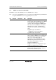
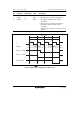
Bit Bit Name Initial Value R/W Description
10 ⎯ 0 R/W Reserved
This bit can be read from or written to. However,
the write value should always be 0.
9
8
RCD1
RCD0
0
0
R/W
R/W
RAS-CAS Wait Control
These bits select a wait cycle to be inserted
between the RAS assert cycle and CAS assert
cycle. A 1- to 4-state wait cycle can be inserted.
00: Wait cycle not inserted
01: 1-state wait cycle inserted
10: 2-state wait cycle inserted
11: 3-state wait cycle inserted
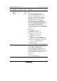
7 to 4 ⎯ All 0 R/W Reserved
These bits can be read from or written to.
However, the write value should always be 0.
3 CKSPE* 0 R/W Clock Suspend Enable
Enables clock suspend mode for extend read data
during DMAC and EXDMAC single address
transfer with the synchronous DRAM interface.
0: Disables clock suspend mode
1: Enables clock suspend mode
2 ⎯ 0 R/W Reserved
This bit can be read from or written to. However,
the write value should always be 0.
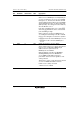
1
0
RDXC1*
RDXC0*
0
0
R/W
R/W
Read Data Extension Cycle Number Selection
Selects the number of read data extension cycle
(Tsp) insertion state in clock suspend mode.
These bits are valid when the CKSPE bit is set to
1.
00: Inserts 1 state
01: Inserts 2 state
10: Inserts 3 state
11: Inserts 4 state
Note: * Not supported by the H8S/2426 Group and H8S/2424 Group.