
Datasheet

Section 6 Bus Controller (BSC)
R01UH0310EJ0500 Rev. 5.00 Page 171 of 1384
Sep 25, 2012
H8S/2426, H8S/2426R, H8S/2424 Group
6.3.9 DRAM Control Register (DRAMCR)
DRAMCR is used to make DRAM/synchronous DRAM interface settings.
Note: The synchronous DRAM interface is not supported by the H8S/2426 Group and H8S/2424
Group. The DRAM interface is not supported by the 5-V version.
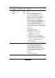
Bit Bit Name Initial Value R/W Description
15 OEE 0 R/W OE Output Enable
The OE signal used when EDO page mode DRAM
is connected can be output. The OE signal is
common to all areas designated as DRAM space.
When the synchronous DRAM is connected, the
CKE signal can be output. The CKE signal is
common to the continuous synchronous DRAM
space.
0: OE/CKE signal output disabled
OE/CKE pin can be used as I/O port.
1: OE/CKE signal output enabled
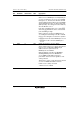
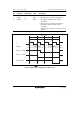
14 RAST 0 R/W RAS Assertion Timing Select
Selects whether, in DRAM access, the RAS signal
is asserted from the start of the T
r
cycle (rising
edge of φ) or from the falling edge of φ.
Figure 6.4 shows the relationship between the
RAST bit setting and the RAS assertion timing.
The setting of this bit applies to all areas
designated as DRAM space.
0: RAS is asserted from φ falling edge in T
r
cycle
1: RAS is asserted from start of T
r
cycle
13 ⎯ 0 R/W Reserved
This bit can be read from or written to. However,
the write value should always be 0.