
Datasheet


Section 6 Bus Controller (BSC)
R01UH0310EJ0500 Rev. 5.00 Page 169 of 1384
Sep 25, 2012
H8S/2426, H8S/2426R, H8S/2424 Group
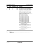
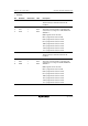
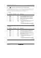
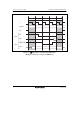
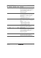
Bit Bit Name Initial Value R/W Description
10 ICIS0 1 R/W Idle Cycle Insert 0
When an external read cycle and external write
cycle are performed consecutively, an idle cycle
can be inserted between the bus cycles.
0: Idle cycle not inserted
1: Idle cycle inserted
9 WDBE 0 R/W Write Data Buffer Enable
The write data buffer function can be used for an
external write cycle or DMAC single address
transfer cycle.
0: Write data buffer function not used
1: Write data buffer function used
8 WAITE 0 R/W WAIT Pin Enable
Selects enabling or disabling of wait input by the
WAIT pin.
0: Wait input by WAIT pin disabled
WAIT pin can be used as I/O port
1: Wait input by WAIT pin enabled
7 to 3 ⎯ All 0 R/W Reserved
These bits can be read from or written to.
However, the write value should always be 0.
2 ICIS2 0 R/W Idle Cycle Insert 2
When an external write cycle and external read
cycle are performed consecutively, an idle cycle
can be inserted between the bus cycles.
0: Idle cycle not inserted
1: Idle cycle inserted
1, 0 ⎯ All 0 R/W Reserved
These bits can be read from or written to.
However, the write value should always be 0.
Note: * The refresh control is not supported by the 5-V version.