
Datasheet


Section 6 Bus Controller (BSC)
R01UH0310EJ0500 Rev. 5.00 Page 161 of 1384
Sep 25, 2012
H8S/2426, H8S/2426R, H8S/2424 Group
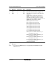
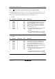
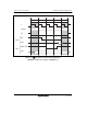
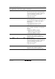
Bit Bit Name Initial Value R/W Description
10
9
8
W22
W21
W20
1
1
1
R/W
R/W
R/W
Area 2 Wait Control 2 to 0
These bits select the number of program wait
states when accessing area 2 while AST2 bit in
ASTCR = 1.
A CAS latency is set when the synchronous
DRAM* is connected. The setting of area 2 is
reflected to the setting of areas 2 to 5. A CAS
latency can be set regardless of whether or not an
ASTCR wait state insertion is enabled.
000: Program wait not inserted
001: 1 program wait state inserted
010: 2 program wait states inserted
011: 3 program wait states inserted
100: 4 program wait states inserted
101: 5 program wait states inserted
110: 6 program wait states inserted
111: 7 program wait states inserted
000: Synchronous DRAM of CAS latency 1 is
connected to areas 2 to 5.
001: Synchronous DRAM of CAS latency 2 is
connected to areas 2 to 5.
010: Synchronous DRAM of CAS latency 3 is
connected to areas 2 to 5.
011: Synchronous DRAM of CAS latency 4 is
connected to areas 2 to 5.
1XX: Setting prohibited.
[Legend]
X: Don't care.
Note: * The synchronous DRAM interface is not supported by the H8S/2426 Group and
H8S/2424 Group.