
Datasheet


Section 6 Bus Controller (BSC)
Page 152 of 1384 R01UH0310EJ0500 Rev. 5.00
Sep 25, 2012
H8S/2426, H8S/2426R, H8S/2424 Group
6.2 Input/Output Pins
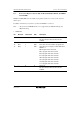
Table 6.1 shows the pin configuration of the bus controller.
Table 6.1 Pin Configuration
Name Symbol I/O Function
Address strobe AS Output Strobe signal indicating that normal space
is accessed and address output on
address bus is enabled.
Address hold AH Output Signal indicating the timing for latching the
address when the address/data
multiplexed I/O space is set.
Read RD Output Strobe signal indicating that normal space
is being read.
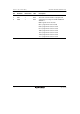
High write/write enable*
1
HWR/WE*
1
Output Strobe signal indicating that normal space
is written to, and upper half (D15 to D8) of
data bus is enabled or DRAM space write
enable signal.
Low write LWR Output Strobe signal indicating that normal space
is written to, and lower half (D7 to D0) of
data bus is enabled.
Chip select 0 CS0 Output Strobe signal indicating that area 0 is
selected.
Chip select 1 CS1 Output Strobe signal indicating that area 1 is
selected
Chip select 2/
row address strobe 2*
1
/
row address strobe*
2
CS2/
RAS2*
1
/
RAS*
2
Output Strobe signal indicating that area 2 is
selected, DRAM row address strobe signal
when area 2 is DRAM space or areas 2 to
5 are set as continuous DRAM space, or
row address strobe signal of the
synchronous DRAM when the
synchronous DRAM interface is selected.
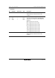
Chip select 3/
row address strobe 3*
1
/
column address strobe*
2
CS3/
RAS3*
1
/
CAS*
2
Output Strobe signal indicating that area 3 is
selected, DRAM row address strobe signal
when area 3 is DRAM space, or column
address strobe signal of the synchronous
DRAM when the synchronous DRAM
interface is selected.