
Datasheet

R01UH0310EJ0500 Rev. 5.00 Page 1377 of 1384
Sep 25, 2012
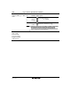
Item Page Revision (See Manual for Details)
Table 25.2 DC
Characteristics (1)
Table 25.27 DC
Characteristics (1)
1216,
1217
1282,
1283
Added and amended
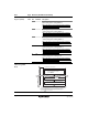
Item
Schmitt trigger
input voltage
Ports 1*
6
and 2*
6
,
P32 to P35*
2
,
P50 to P53*
2
,
ports 6*
2
and 8*
2
,
PA4 to PA7*
2
,
ports B*
2
and C*
2
,
PF1*
2
, PF2*
2
,
PH2*
2
, PH3*
2
Input high voltage P14 to P17*
5
,
P24 to P26*
5
,
port 3*
3
,
P50 to P53*
3
,
ports 6*
3
and 8*
3
,
ports A to J*
3
Input low voltage P14 to P17*
5
,
P24 to P26*
5
,
ports 3*
3
, 5*
3
, and 6*
3
,
port 8*
3
,
ports A to J*
3
Notes: 5. When used as SSO, SSI, SSCK, SCS, WAIT, or ADTRG1.
6. When used as other than SSO, SSI, SSCK, SCS, WAIT, or
ADTRG1.
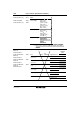
Table 25.13 Flash
Memory
Characteristics
Table 25.25 Flash
Memory
Characteristics
Table 25.38 Flash
Memory
Characteristics
Table 25.50 Flash
Memory
Characteristics
1230
1246
1295
1310
Deleted and amended
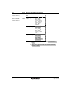
Standard
Value
Item Symbol
Test
Conditions Applicable Area Max.
Programming ROM ⎯ Programming and
erase count*
1
Data flash area ⎯
Programming ROM 4000 Programming time
(per 4 bytes)
Data flash area
4000
Programming ROM 3000 Erase time (per 1
block)
Data flash area
3000
Programming ROM Programming and
erase voltage
Data flash area
3.6
Programming ROM Read voltage
Data flash area
3.6
Programming ROM ⎯ Access state
Data flash area ⎯