
Datasheet

Page 1376 of 1384 R01UH0310EJ0500 Rev. 5.00
Sep 25, 2012
Item Page Revision (See Manual for Details)
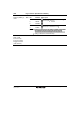
19.3.5 SS Status
Register (SSSR)
1045,
1046
Deleted
Bit Bit Name Description
6 ORER [Clearing condition]
When writing 0 after reading ORER = 1
(When the CPU is used to clear this flag by writing 0
hile the corresponding interrupt is enabled, be sure to
ead the flag after writing 0 to it.)
3 TEND [Clearing condition]
• When writing 0 after reading TEND = 1
(When the CPU is used to clear this flag by writing 0
while the corresponding interrupt is enabled, be sure to
read the flag after writing 0 to it.)
2 TDRE [Clearing condition]
• When writing 0 after reading TDRE = 1
(When the CPU is used to clear this flag by writing 0
while the corresponding interrupt is enabled, be sure to
read the flag after writing 0 to it.)
1 RDRF [Clearing condition]
• When writing 0 after reading RDRF = 1
(When the CPU is used to clear this flag by writing 0
while the corresponding interrupt is enabled, be sure to
read the flag after writing 0 to it.)
0 CE [Clearing condition]
• When writing 0 after reading CE = 1
(When the CPU is used to cl
ear this flag by writing 0
while the corresponding interrupt is enabled, be sure to
read the flag after writing 0 to it.)
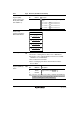
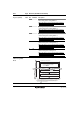
Figure 21.2 Setting
and Clearing EW0
Mode
1086 Amended
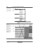
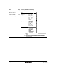
Jump to a desired address in the flash memory.
Programming control program*
4
Write 0 to the FMCMDEN bit and then write 1
to it (user program mode enabled).*
1
Clear CBIDB to 0.
Write 1 to the CBIDB bit (user program mode
disabled).
1.
2.
3.
To set the FMCMDEN bit to 1, write 0 to the bit and then write 1 to it in a row.
Write to the FMCMDEN bit from an area outside the on-chip flash memory.
After a read array command, disable user programming mode.
In user program mode, execute the programming control program in
the on-chip RAM or external area.
Notes: