
Datasheet

Page 1374 of 1384 R01UH0310EJ0500 Rev. 5.00
Sep 25, 2012
Item Page Revision (See Manual for Details)
15.3.7 Serial Status
Register (SSR)
Smart Card Interface
Mode (When SMIF
bit in SCMR is 1)
887 Amended
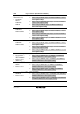
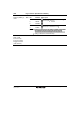
Bit Bit Name Description
2 TEND Timing to set this bit differs according to the register
settings.
GM = 0, BLK = 0: 12.5 etu after transmission
GM = 0, BLK = 1: 11.5 etu after transmission
GM = 1, BLK = 0: 11.0 etu after transmission
GM = 1, BLK = 1: 11.0 etu after transmission
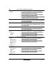
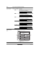
Table 15.2
Relationships
between N Setting in
BRR and Bit Rate B
889
Amended and added
Bit Rate
N =− 1
64 × 2
2n−1
× B
φ × 10
6
− 1N =
32 × 2
2n−1
× B
φ × 10
6
− 1N =
8 × 2
2n−1
× B
φ × 10
6
− 1N =
S × 2
2n+1
× B
φ × 10
6
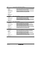
16.7 Usage Notes 989,
990
Added
5. Restriction on Setting Transfer Rate in Use of Multi-Master
6. Restriction on Use of Bit Manipulation Instructions to Set MST
and TRS in Use of Multi-Master
7. Note on Master Receive Mode
8. Notes on Changing from Master Transmit Mode to Master
Receive Mode
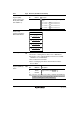
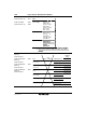
17.3.4 A/D Control
Register (ADCR_0)
Unit 0
1004,
1005
Added
Bit Bit Name Description
7
6
0
TRGS1
TRGS0
EXTRGS
010: Enables A/D conversion start by external
trigger from TPU (units 0 and 1)*
Note: * If this bit is set the same as the TRGS_1, TRGS0, and EXTRGS bits
in ADCR_1, the A/D converter units 0 and 1 start A/D conversion by
conversion start trigger from TPU (units 0 and 1).