
Datasheet


R01UH0310EJ0500 Rev. 5.00 Page 1363 of 1384
Sep 25, 2012
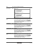
Main Revisions and Additions in this Edition
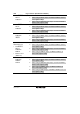
Item Page Revision (See Manual for Details)
4.3 Reset 98 Amended
A reset has the highest exception priority. When the RES pin goes
low, all processing halts and this LSI enters the reset. To ensure
that this LSI is reset, hold the RES pin low for at least 15 ms at
power-up. To reset this LSI during operation, hold the RES pin low
for at least 2 ms.
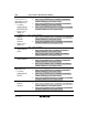
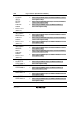
7.1 Features 315 Amended
• Activation sources: internal interrupt, external request, auto-
request (depending on transfer mode)
⎯ Six compare match/input capture interrupts of 16-bit timer-
pulse unit (TPU0 to 5).
⎯ Transmit data empty and receive data full interrupts of serial
communication interface (SCI_0, SCI_1)
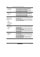
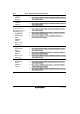
7.3.4 DMA Control
Registers (DMACRA
and DMACRB)
(1) Short Address
Mode:
• DMACR_0A,
DMACR_0B,
DMACR_1A, and
DMARC_1B
325,
326
Amended
Bit Bit Name Description
3
2
1
0
DTF3
DTF2
DTF1
DTF0
• Channel A
0100: Activated by SCI channel 0 transmit data empty interrupt
0101: Activated by SCI channel 0 receive data full interrupt
0110: Activated by SCI channel 1 transmit data empty interrupt
0111: Activated by SCI channel 1 receive data full interrupt
• Channel B
0100: Activated by SCI channel 0 transmit data empty interrupt
0101: Activated by SCI channel 0 receive data full interrupt
0110: Activated by SCI channel 1 transmit data empty interrupt
0111: Activated by SCI channel 1 receive data full interrupt
(2) Full Address
Mode
• DMACR_0B and
DMACR_1B
330 Amended
Bit Bit Name Description
3
2
1
0
DTF3
DTF2
DTF1
DTF0
• Block Transfer Mode
0100: Activated by SCI channel 0 transmit data empty interrupt
0101: Activated by SCI channel 0 receive data full interrupt
0110: Activated by SCI channel 1 transmit data empty interrupt
0111: Activated by SCI channel 1 receive data full interrupt