
Datasheet


Appendix
R01UH0310EJ0500 Rev. 5.00 Page 1361 of 1384
Sep 25, 2012
H8S/2426, H8S/2426R, H8S/2424 Group
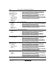
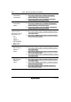
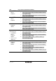
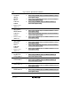
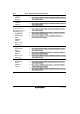
Pin Name Mode 1 Mode 2 Mode 4 Mode 7
PF7
• This pin is left open in the initial state for the φ output.
PF6
• This pin is left open in the initial state for the AS output.
PF5
• This pin is left open in the initial state for the RD output.
PF4
• This pin is left open in the initial state for the HWR
output.
PF3
• This pin is left open in the initial state for the LWR
output.
PG0
• This pin is left open in the initial
state for the CS0 output.
PA4 to PA0
Port B
Port C
• These pins are left open in the
initial state for the address output.
• Connect these
pins to V
CC
via a
pull-up resistor or
to V
SS
via a pull-
down resistor,
respectively
PH1
• This pin is left open in the initial state for the SDRAM0
output. (H8S/2426R)
• Connect this pin to V
CC
via a pull-up resistor or to V
SS
via
a pull-down resistor, respectively. (H8S/2426 and
H8S/2424)