
Datasheet


Appendix
Page 1360 of 1384 R01UH0310EJ0500 Rev. 5.00
Sep 25, 2012
H8S/2426, H8S/2426R, H8S/2424 Group
C. Treatment of Unused Pins
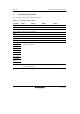
The treatments of unused pins are listed in table C.1
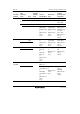
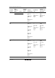
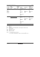
Table C.1 Treatment of Unused Pins
Pin Name Mode 1 Mode 2 Mode 4 Mode 7
RES
• Connect this pin to V
CC
via a pull-up resistor
STBY
• Connect this pin to V
CC
via a pull-up resistor
EMLE
• Connect this pin to V
SS
via a pull-down resistor
MD2 to MD0 (Always used as mode pins)
NMI
• Connect this pin to V
CC
via a pull-up resistor
EXTAL (Always used as a clock pin)
XTAL
• Leave this pin open
WDTOVF
• Leave this pin open
Port 1
Port 2
Port 3
Port 5
Port 8
PA7 to PA5
PF2 to PF0
PG7 to PG1
PH3, PH2,
PH0
PJ2 to PJ0
• Connect these pins to V
CC
via a pull-up resistor or to V
SS
via a pull-down
resistor, respectively
Ports 4 and 9
• Connect these pins to AV
CC
via a pull-up resistor or to AV
SS
via a pull-down
resistor, respectively