
Datasheet


Section 25 Electrical Characteristics
Page 1300 of 1384 R01UH0310EJ0500 Rev. 5.00
Sep 25, 2012
H8S/2426, H8S/2426R, H8S/2424 Group
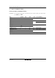
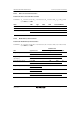
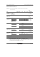
Table 25.41 DC Characteristics (2)
Conditions: V
CC
= 4.5 V to 5.5 V, AV
CC
= 4.5 V to 5.5 V, V
ref
= 4.5 V to AV
CC
,
V
SS
= AV
SS
= 0 V*
1
Item Symbol Min. Typ. Max. Unit
Test
Conditions
Three-state
leakage current
(off state)
Ports 1 to 3,
P50 to P53,
port 8,
ports A to G
| I
TSI
| ⎯ ⎯ 1.0 μA V
in
= 0.5 to
V
CC
−0.5 V
Input pull-up
MOS current
Ports A to E −I
p
10 ⎯ 300 μA V
CC
= 4.0 to
5.5 V
V
in
= 0 V
RES ⎯ ⎯ 30 pF
NMI ⎯ ⎯ 30 pF
Input
capacitance
All input pins
except RES and
NMI
C
in
⎯ ⎯ 18 pF
V
in
= 0 V
f = 1 MHz
T
a
= 25°C
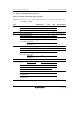
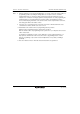
Normal operation ⎯ 45
(5.0 V)
70 mA f = 33 MHz
Sleep mode ⎯ 35
(5.0 V)
45 mA f = 33 MHz
⎯ 20 80 μA T
a
≤ 50°C
Supply current*
2
Standby mode*
3
I
CC
*
4
⎯ 80 500 μA 50°C < T
a
During A/D and
D/A conversion
⎯ 0.5
(5.0 V)
2.0 mA When channel
1 is in use
Analog power
supply current
Idling
AI
CC
⎯ 0.01 5.0 μA When channel
1 is in use
During A/D and
D/A conversion
⎯ 0.5
(5.0 V)
1.0 mA Reference
power supply
current
Idling
AI
CC
⎯ 0.01 5.0 μA
RAM standby voltage V
RAM
2.5 ⎯ ⎯ V
V
CC
start voltage*
5
V
CC start
⎯ ⎯ 0.3 V
V
CC
rising slope *
5
SV
CC
⎯ ⎯ 20 ms/V
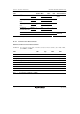
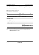
Notes: 1. When the A/D and D/A converters are not used, the AV
CC
, V
ref
, and AV
SS
pins should not
be open. Connect the AV
CC
and V
ref
pins to V
CC
, and the AV
SS
pin to V
SS
.
2. Supply current values are for V
IH
min = V
CC
−0.2 V and V
IL
max = 0.2 V with all output pins
unloaded and all input pull-up MOSs in the off state.