
Datasheet


Section 25 Electrical Characteristics
Page 1290 of 1384 R01UH0310EJ0500 Rev. 5.00
Sep 25, 2012
H8S/2426, H8S/2426R, H8S/2424 Group
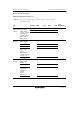
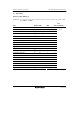
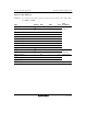
Table 25.33 Bus Timing (2)
Conditions: V
CC
= 4.5 V to 5.5 V, AV
CC
= 4.5 V to 5.5 V, V
ref
= 4.5 V to AV
CC
, V
SS
= AV
SS
= 0 V,
φ = 8 MHz to 33 MHz
Item Symbol Min. Max. Unit
Test
Conditions
WR delay time 1 t
WRD1
⎯ 15 ns
WR delay time 2 t
WRD2
⎯ 15 ns
WR pulse width 1 t
WSW1
1.0 × t
cyc
−13 ⎯ ns
WR pulse width 2 t
WSW2
1.5 × t
cyc
−13 ⎯ ns
Figures 25.58
to 25.73
Write data delay time t
WDD
⎯ 23 ns
Write data setup time 1 t
WDS1
0.5 × t
cyc
−15 ⎯ ns
Write data setup time 2 t
WDS2
1.0 × t
cyc
−15 ⎯ ns
Write data setup time 3 t
WDS3
1.5 × t
cyc
−15 ⎯ ns
Write data hold time 1 t
WDH1
0.5 × t
cyc
−13 ⎯ ns
Write data hold time 3 t
WDH3
1.5 × t
cyc
−13 ⎯ ns
WAIT setup time t
WTS
25 ⎯ ns
WAIT hold time t
WTH
1 ⎯ ns
Figures 25.60
and 27.73
BREQ setup time t
BREQS
30 ⎯ ns
BACK delay time t
BACD
⎯ 15 ns
Bus floating time t
BZD
⎯ 40 ns
Figure 25.65
BREQO delay time t
BRQOD
⎯ 25 ns Figure 25.66