
Datasheet

Section 25 Electrical Characteristics
R01UH0310EJ0500 Rev. 5.00 Page 1287 of 1384
Sep 25, 2012
H8S/2426, H8S/2426R, H8S/2424 Group
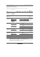
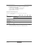
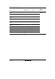
LSI output pin
CRH
RL
3V
C=50pF: Ports A to J
C=30pF: Ports 1 to 3, P50 to P52, and ports 6 and 8.
RL=2.4kΩ
RH=12kΩ
Output timing test level 2.5V: (Vcc=4.5 to 5.5V)
Figure 25.52 Output Load Circuit
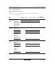
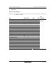
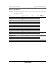
(2) Control Signal Timing
Table 25.31 Control Signal Timing
Conditions: V
CC
= 4.5 V to 5.5 V, AV
CC
= 4.5 V to 5.5 V, V
ref
= 4.5 V to AV
CC
, V
SS
= AV
SS
= 0 V,
φ = 8 MHz to 33 MHz
Item Symbol Min. Max. Unit Test Conditions
RES setup time t
RESS
200 ⎯ ns Figure 25.56
RES pulse width t
RESW
2 ⎯ ms
NMI setup time t
NMIS
150 ⎯ ns Figure 25.57
NMI hold time t
NMIH
10 ⎯
NMI pulse width (in recovery from
software standby mode)
t
NMIW
200 ⎯
IRQ setup time t
IRQS
150 ⎯ ns
IRQ hold time t
IRQH
10 ⎯
IRQ pulse width (in recovery from
software standby mode)
t
IRQW
200 ⎯