
Datasheet


Section 25 Electrical Characteristics
R01UH0310EJ0500 Rev. 5.00 Page 1243 of 1384
Sep 25, 2012
H8S/2426, H8S/2426R, H8S/2424 Group
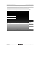
Item Symbol Min. Max. Unit Test Conditions
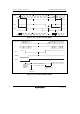
8-bit timer Timer output delay time t
TMOD
⎯ 40 ns Figure 25.40
Timer reset input setup time t
TMRS
25 ⎯ ns Figure 25.42
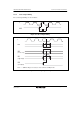
Timer clock input setup time t
TMCS
25 ⎯ ns Figure 25.41
Timer clock
pulse width
Single-edge
specification
t
TMCWH
1.5 ⎯ t
cyc
Both-edge
specification
t
TMCWL
2.5 ⎯ t
cyc
WDT Overflow output delay time t
WOVD
⎯ 40 ns Figure 25.43
SCI Asynchronous t
Scyc
4 ⎯ t
cyc
Figure 25.44
Input clock
cycle
Synchronous 6 ⎯
Input clock pulse width t
SCKW
0.4 0.6 t
Scyc
Input clock rising time t
SCKr
⎯ 1.5 t
cyc
Input clock falling time t
SCKf
⎯ 1.5
Transmit data delay time t
TXD
⎯ 40 ns Figure 25.45
Receive data setup time
(synchronous)
t
RXS
40 ⎯ ns
Receive data hold time
(synchronous)
t
RXH
40 ⎯ ns
A/D
converter
Trigger input setup time t
TRGS
30 ⎯ ns Figure 25.46
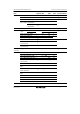
IIC2 SCL input cycle time t
SCL
12 t
cyc
+600 ⎯ ns Figure 25.47
SCL input high pulse width t
SCLH
3 t
cyc
+300 ⎯ ns
SCL input low pulse width t
SCLL
5 t
cyc
+300 ⎯ ns
SCL, SDA Input falling time t
Sf
⎯ 300 ns
SCL, SDA Input spike pulse
removal time
t
SP
⎯ 1 t
cyc
ns
SDA input bus free time t
BUF
5 t
cyc
⎯ ns
Start condition input hold
time
t
STAH
3 t
cyc
⎯ ns
Retransmit start condition
input setup time
t
STAS
3 t
cyc
⎯ ns
Stop condition input setup
time
t
STOS
3 t
cyc
⎯ ns
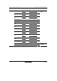
Data input setup time t
SDAS
1 t
cyc
+20 ⎯ ns
Data input hold time t
SDAH
0 ⎯ ns
SCL, SDA capacitive load Cb ⎯ 400 pF
SCL, SDA falling time t
Sf
⎯ 300 ns