
Datasheet


Section 25 Electrical Characteristics
Page 1242 of 1384 R01UH0310EJ0500 Rev. 5.00
Sep 25, 2012
H8S/2426, H8S/2426R, H8S/2424 Group
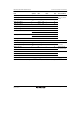
(4) DMAC Timing
Table 25.21 DMAC Timing
Conditions: V
CC
= 3.0 V to 3.6 V, AV
CC
= 3.0 V to 3.6 V, V
ref
= 3.0 V to AV
CC
, V
SS
= AV
SS
= 0 V,
φ = 8 MHz to 33 MHz
Item Symbol Min. Max. Unit Test Conditions
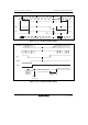
DREQ setup time t
DRQS
25 ⎯ ns Figure 25.32
DREQ hold time t
DRQH
10 ⎯
TEND delay time t
TED
⎯ 18 Figure 25.31
DACK delay time 1 t
DACD1
⎯ 18 Figures 25.29 and 25.30
DACK delay time 2 t
DACD2
⎯ 18
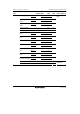
(5) Timing of On-Chip Peripheral Modules
Table 25.22 Timing of On-Chip Peripheral Modules
Conditions: V
CC
= 3.0 V to 3.6 V, AV
CC
= 3.0 V to 3.6 V, V
ref
= 3.0 V to AV
CC
, V
SS
= AV
SS
= 0 V,
φ = 8 MHz to 33 MHz
Item Symbol Min. Max. Unit Test Conditions
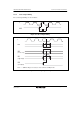
I/O ports Output data delay time t
PWD
⎯ 40 ns Figure 25.36
Input data setup time t
PRS
25 ⎯ ns
Input data hold time t
PRH
25 ⎯ ns
PPG Pulse output delay time t
POD
⎯ 40 ns Figure 25.37
TPU Timer output delay time t
TOCD
⎯ 40 ns Figure 25.38
Timer input setup time t
TICS
25 ⎯ ns
Timer clock input setup time t
TCKS
25 ⎯ ns Figure 25.39
Timer clock
pulse width
Single-edge
specification
t
TCKWH
1.5 ⎯ t
cyc
Both-edge
specification
t
TCKWL
2.5 ⎯ t
cyc