
Datasheet


Section 25 Electrical Characteristics
R01UH0310EJ0500 Rev. 5.00 Page 1237 of 1384
Sep 25, 2012
H8S/2426, H8S/2426R, H8S/2424 Group
25.2.3 AC Characteristics
The following shows the timings of the clock, control signals, bus, DMAC, and on-chip peripheral
functions.
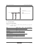
(1) Clock Timing
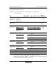
Table 25.18 Clock Timing
Conditions: V
CC
= 3.0 V to 3.6 V, AV
CC
= 3.0 V to 3.6 V, V
ref
= 3.0 V to AV
CC
, V
SS
= AV
SS
= 0 V,
φ = 8 MHz to 33 MHz
Item Symbol Min. Max. Unit Test Conditions
Clock cycle time t
cyc
30.3 125 ns Figure 25.3
Clock pulse high width t
CH
10 ⎯ ns Figure 25.3
Clock pulse low width t
CL
10 ⎯ ns
Clock rising time t
Cr
⎯ 5 ns
Clock falling time t
Cf
⎯ 5 ns
Reset oscillation settling time
(crystal)
t
OSC1
15 ⎯ ms Figure 25.5(1)
Software standby oscillation
settling time (crystal)
t
OSC2
5 ⎯ ms Figure 25.5(2)
External clock output delay
settling time
t
DEXT
15 ⎯ ms Figure 25.5(1)